

Electro mobility, automation, autonomous driving, 5G-communication and Industry 4.0 are major current trends which, in many areas of life, go hand-in-hand with extensive digitalization. All of these require electronic solutions and increasing computing capacity in systems and equipment. For the developers and manufacturers of corresponding technology, this means great potential and well-filled order books. At the same time, the challenges involved in the electronics manufacturing process are increasing all the time, and the spectrum of assemblies and circuit boards is becoming more complex every day. This results in a rise in the challenges faced in the area of electronic module reworking and repairs. New concepts and automated systems are required.
As a specialist for electronics production equipment, Ersa has been involved in the professional reworking of modules since as early as the late 1990s. Back then, when the Ball Grid Array (BGA) was still a relatively new type of packaging for integrated circuits, the expertise was developed for selective processing of this kind of surface mounted device in rework.
Today, a good 25 years later, BGAs are among the indispensable elements in modern, high-performance electronics. They have become standard in some fields, have already been partially replaced by more modern, more economical designs in others, and it is impossible to imagine the area of high-performance electronics without them. In 5G applications, BGAs with an edge length of up to 110 x 110mm and a grid dimension of 0.6 mm to 1.0 mm are used. A single assembly has up to 12,100 solder balls.
At the other end of the assembly scale, we find the tiniest of electronic circuits: Still indispensable today are passive, discreet, two-pin SMD assemblies. 01005 chip condensers or resistances with dimensions of 0.4 x 0.2 mm have become common, and ever smaller versions are already in use.
The spectrum of assembly forms between these critical values is practically continuous. The challenge for electronics manufacturing is therefore to be able to process all assemblies in the line process and to have corresponding repair concepts available where faults occur.


Defects occur in the manufacturing process, as experts in the branch will always be able to confirm. While system and processing engineering has become steadily more sophisticated in all areas of manufacturing over recent years, new challenges have continued to regularly emerge over the same period. Ever-decreasing grid dimensions or rising complexity of the circuits are just two examples.
Solder paste printing, for example, is still responsible for many of the soldering defects on SMT modules. Only with state-of-the-art stencil printers, a sophisticated stencil technique (e.g. multi-stage stencils) and integrated 3D inspection can print errors be recognised and corrected inline. Placement errors or the use of incorrect assemblies and many further factors mean that the “zero error” production target cannot always be achieved.
Depending on the size and nature of the module, all electronics can be successfully reworked today. As a result, solder joints that match the quality of the fault-free manufacturing process can be expected. Lastly, the “Guide to reworking electronic modules” (Leitfaden Rework elektronischer Module) of the ZVEI confirms that reworking processes can be executed in a computable and reliable way.
The assembly forms mentioned above are in use today on very small modules (e.g. hearing aids) or extremely large ones (server boards, 5G modules). The demands made of the repair process are rising accordingly.
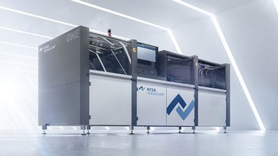
With the current Ersa rework systems, modules with dimensions of up to 625 x 1250 mm (24 x 48 inch) can be processed. The now very high level of automation of these systems guarantees a high degree of both process reliability and reproducibility in reworking.
Regardless of whether a 01005 or a large BGA is involved: The assemblies are received for placement by the Ersa rework system, automatically aligned by image processing, deposited in the target position and then soldered.
For the processing of chip assemblies, the Ersa HR 600/3P offers very fine nozzles and belt transportation. With the aid of the dip-transfer process, it is even possible to replenish the solder paste depot for these miniature assemblies. Here a transfer needle conveys solder paste from the reservoir to the soldering point.
In both the large BGA and the Land Gird Array (LGA) assemblies, identification of the connection also takes place fully automatically. With the aid of the Dip&Print Station, the assembly conncetions can be immersed automatically in the fluxing agent or printed with solder paste using a suitable stencil. Because the correct solder volume is decisive for the quality of the soldering. While, as a rule, chips can be easily desoldered and soldered into place, large assemblies can require both a larger heating head and greater pulling force when desoldering. A very high-performance vacuum system in the Ersa HR 600 XL with large nozzles or double nozzles is the right solution here.
Particularly in the case of large circuit boards, homogenous warming of the module can be of special significance: due to the coefficient of thermal expansion of the materials involved, large circuit boards tend to become distorted during the warming process. A cleverly-designed heating technology ensures homogenous warming with minimum distortion: the IR Matrix lower heating in the HR 600 XL can bring the module up to the required temperature with 25 individually-selectable heating elements, individually optimised. For example, the edges of the circuit boards can be heated to a higher temperature than the centre, or individual areas of the circuit boards can be heated to a lower temperature than others (“cold spot”). Supporting elements in the PCB frame keep the circuit boards firmly in position during the process and prevent flection.
In the profile-controlled soldering process, the system heating of the Ersa Hybrid rework system follows the readings of the controlling pot sensor on the circuit boards and automatically ensures a reproducible result for this process. External influences are registered and taken into account in the adjustments. In addition, by means of the reflow process camera on the equipment, the system user has a clear view of the solder joint, therefore always retaining an overview of the process.
Ersa has the comprehensive process expertise gained in line processes to be able to offer the right rework solutions for reworking modern modules. From 01005 to 625 x 1.250 mm!

![[Translate to English:]](/fileadmin/_processed_/7/9/csm_Titel_1920x850px-74_144f2e9e35.jpg "[Translate to English:]")